Electron Flow in a High Mobility Two Dimensional Electron Gas
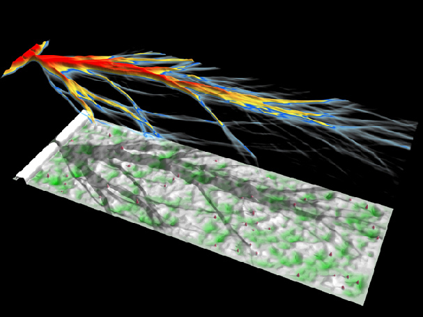
Electron motion through high mobility two dimensional electron gases is often thought to be nearly ideal. As shown in the figure, Heller has discovered that electron flow from a quantum point contact forms narrow channels at distances well below the mean free path. The upper part of the figure shows the computed electron wave flow over the potential shown in the lower part (high potential is white, low is green). These calculations agree well with images of electron flow from a quantum point contact in a GaAs/AlGaAs heterostructure obtained by scanned probe microscopy at low temperatures by Westervelt. Although the statistically averaged parameters - mobility, mean free path - are the same as traditional pictures, the actual flow through a given nanoscale device shows additional structure. These developments improve our picture of electron flow, with important effects on nanoscale electronic device design.
Heller and Westervelt
Harvard MRSEC (DMR-0820484)